PCIe Bifurcation
LattePanda Mu Ultra x86 compute module exposes 8 dedicated PCIe 4.0 lanes. These lanes are PCIe only — they cannot be reconfigured as USB 3.2 or SATA.
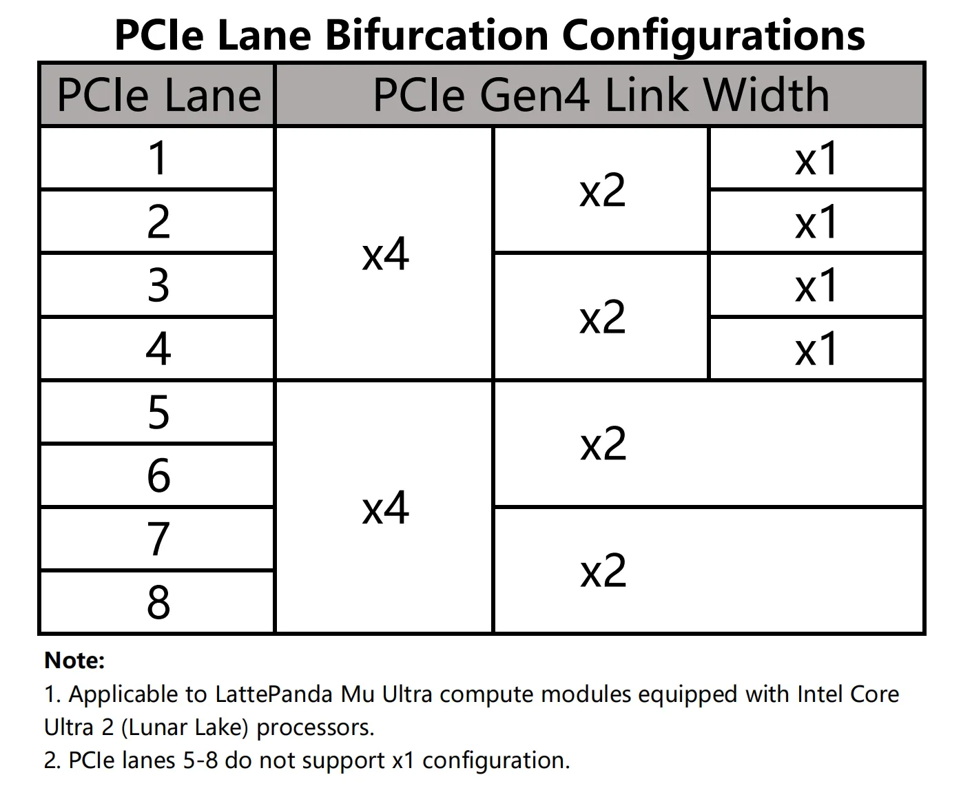
Bifurcation Configuration
Rules
The 8 PCIe lanes are divided into two groups with different bifurcation capabilities:
- PCIe Lanes 1 ~ 4: Support flexible bifurcation down to independent x1 links.
- PCIe Lanes 5 ~ 8: Can only be bifurcated down to x2 — x1 is not supported on these lanes.
Overall, the following configurations are supported:
-
Up to 4× PCIe 4.0 x1
Lane1 (x1) + Lane2 (x1) + Lane3 (x1) + Lane4 (x1)
-
Up to 4× PCIe 4.0 x2
Lane1+2 (x2) + Lane3+4 (x2) + Lane5+6 (x2) + Lane7+8 (x2)
-
Up to 2× PCIe 4.0 x4
Lane1+2+3+4 (x4) + Lane5+6+7+8 (x4)
If your design requires multiple independent x1 devices (e.g., several PCIe Ethernet controllers), place them on Lanes 1–4.
Key Differences from LattePanda Mu
| LattePanda Mu | LattePanda Mu Ultra | |
|---|---|---|
| Lane Source | HSIO multiplexing (PCIe/USB 3.2/SATA) | Dedicated PCIe lanes |
| PCIe Generation | PCIe 3.0 (8.0 GT/s) | PCIe 4.0 (16 GT/s) |
| Number of Lanes | 9 | 8 |
| Bifurcation Limit | Down to x1 on all lanes | Lanes 1-4: down to x1 Lanes 5–8: down to x2 only |
PCIe Clock Distribution
The LattePanda Mu Ultra compute module exposes 5 independent PCIe REFCLKs (REFCLK0–REFCLK4), and all five clock request pins (REFCLK_REQ0#–REFCLK_REQ4#) are available.
CLKREQ Mapping & Control
These pins strictly control specific reference clock output:
- Fixed Mapping: There is a 1-to-1 correspondence, e.g.
CLKREQ3controls onlyREFCLK3, andCLKREQ4controls onlyREFCLK4. This mapping is immutable, e.g., CLKREQ3 cannot be configured to control other clocks. - Control Logic: When a PCIe device drives the
CLKREQpin low, the correspondingREFCLKoutput is enabled. If the pin is released high, the clock output stops.
Clock-to-Lane Mapping
The default BIOS defines a specific binding between the PCIe Clock Outputs (REFCLK) and PCIe Lanes.
| PCIe Lane | Link Width Configuration | Associated REFCLK |
|---|---|---|
| PCIe Lane #3 | PCIe 4.0 x1 | REFCLK0 |
| PCIe Lane #4 | PCIe 4.0 x1 | REFCLK3 |
| PCIe Lane #5 | PCIe 4.0 x4 (Lane 0) | REFCLK2 |
| PCIe Lane #6 | PCIe 4.0 x4 (Lane 1) | Shared with REFCLK2 |
| PCIe Lane #7 | PCIe 4.0 x4 (Lane 2) | Shared with REFCLK2 |
| PCIe Lane #8 | PCIe 4.0 x4 (Lane 3) | Shared with REFCLK2 |
| PCIe Lane #1 | PCIe 4.0 x2 (Lane 0) | REFCLK4 |
| PCIe Lane #2 | PCIe 4.0 x2 (Lane 1) | Shared with REFCLK4 |
Note
To modify the clock-to-lane mapping, customized BIOS firmware is required. It cannot be changed via the BIOS setup menu.
Strict Mapping Required for RTL8111H NIC
Our testing shows that the RTL8111H network controller (NIC) has strict requirements for Clock-to-Lane Mapping, and a mismatch can cause Blue Screen errors in Windows OS.
Example: The RTL8111H chip is connected to PCIe Lane #4. When using the default BIOS firmware, it must use REFCLK3. Manually forcing a different REFCLK output may cause the system to crash.
Action required: For such devices, strictly adhere to the Clock-to-Lane Mapping requirements, or use customized firmware that matches the actual mapping of your carrier board.
CLKREQ Is Mandatory for Modern Standby
-
Every PCIe device must have its CLKREQ pin connected to the corresponding REFCLK_REQ pin. Entering Modern Standby requires PCIe peripherals to use CLKREQ to trigger their low-power state; a device without CLKREQ connected will prevent the system from entering Modern Standby.
-
Do NOT pull CLKREQ permanently low with a pull-down resistor to force an always-on clock (a practice sometimes used on the LattePanda Mu). On the Mu Ultra, a permanently asserted CLKREQ also blocks Modern Standby entry.
-
Some connectors — such as OCuLink connectors or standard PCIe slots — do not carry a CLKREQ pin. Devices attached through these connectors will block Modern Standby.
Applying Configuration Changes
Any change to the PCIe bifurcation configuration or the REFCLK-to-lane mapping requires customized BIOS firmware. These settings cannot be changed dynamically through the BIOS Setup menu. Ensure that the firmware configuration matches the carrier board's actual lane and clock connections.